Two-Port Electronic Load
Link to repository
The motivation for this project came when designing battery management circuits. I needed a way to test that in an over-current state the system would protect the batteries, and that the over-current level was as designed. Using parallel and series combinations of resistors is impractical for this, so a controllable load was the obvious solution. These electronic loads exist commercially, but one annoyance I have with them is that they require external power– to me, it seems that the logic/control could be powered via the source and be a true two-port device.
The design is based around a current-controlled feedback loop where an Op Amp controls the gate voltage on a MOSFET such that the current through a shunt resistor is held constant.
As per usual, I decided to add mostly-unnecessary challenges to make it fun, and instead of using a potentiometer to control the level of current draw, I used an R2R ladder and 8 DIP switches. This allows the current to be reset to precise values with consistency. A 10-Turn potentiometer with a dial would probably be a better fit.
Future designs will likely include a microcontroller that measures the full current sourced (including powering the microcontroller/regulators, etc.) and have a wider input voltage range and have modes such as constant power or constant resistance by measuring the input voltage. A display of current input current and voltage would also be nice, even if it is just an LED array.
Circuit Described
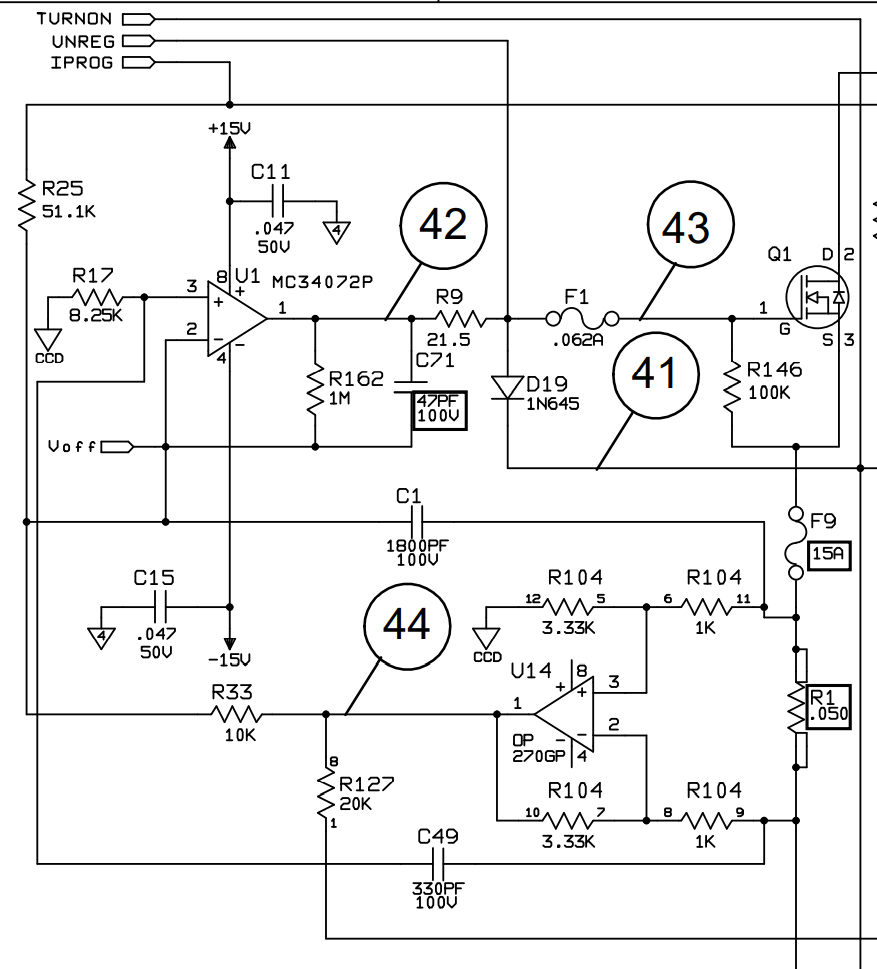
The premise behind the control is very similar to the HP6060B DC electronic load (attached). In that system, there is an N-Ch MOSFET with a 50mOhm source resisor that leads into a differential amplifier (U14) with a voltage gain of 4.33 (1+3.33k/1k), and therefore a total DC gain of 50 x 4.33=0.21V/A at node 44. The input to the non-inverting terminal of U1 has a voltage division of 8.25/(10+8.25), and the current programming voltage(IPROG) at the inverting terminal. So, for example, if the IPROG is above the voltage at the non-inverting input (indicating current is too high) the output voltage of the opamp will go down (because the + input is below the - input) increasing the drain-source impedance of the MOSFET therefore lowering current.
My understanding is that if “TURNON” is pulled low it will ensure all of the MOSFET gates are shut off because the diode D19 will clamp the voltage low. I’m not sure what the purpose of “UNREG” is.
I image R9 is there for stability purposes.
My design is very similar as can be seen in my schematic– the differences are because I designed my system prior to seeing the HP6060B’s design.
** Thermal Considerations**
Obviously, the point of the load is to dissipate energy, so the MOSFETS will overheat if not attached to sufficient heat sinks. For now, I’m only using this for relatively low power applications, so the TO-220 package attached to a small commercial heat-sink is more than sufficient. Before the system is used in a higher power application a more rigorous analysis should be done.